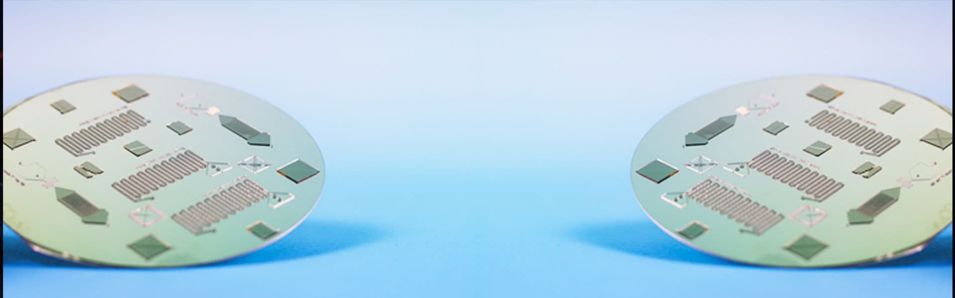
Researchers have mainly oriented themselves towards polymers such as PDMS to make their microfluidic devices. However, it was indeed with glass and silicon that the first microfluidic devices were created, i.e. for liquid and gas chromatography. These materials have many advantages for a wide range of applications.
We will compare 3 microfabrication processes that make it possible to transform these materials into microfluidic devices: surface micromachining, buried channel techniques and bulk micromachining.
Surface micromachining
The surface micromachining technique consists of the use of a sacrificial layer which is shaped to define the desired fluid channels, then a structural layer is deposited and finally the sacrificial layer is etched. It should be noted that although surface micromachining offers greater potential for the fabrication of multilayer devices compared to mass micromachining, it nevertheless involves more process steps per layer. A number of promising surface micromachined microfluidic devices have been reported [James CD et al. 2006 J Micromech Microeng]. Surface micromachining is particularly interesting for the fabrication of nano-channels. Indeed, the thickness of the sacrificial layer that corresponds to the final height of the channel can easily be controlled to the nearest nanometre. Bulk micromachining, on the other hand, cannot offer such channel height control due to spatial variations in etching speed.
Buried channel technology
In buried channel technology, the idea is to create a deep access trench by direct anisotropic deep reactive ion etching (DRIE) of silicon. The side walls are passivated by chemical vapour deposition (CVD), and a circular channel is then isotropically etched, with the bottom of the access trench centrally located [Paick SJ et al. Sens Actuators A]. Moreover, this technology is successful when very deep and narrow access features are used. This requires micron-scale lithography and a high aspect-ratio DRIE.
A variant of this technique is also widely used: DRIE’s isotropic method is used to etch bulk silicon under a perforated silicon nitride mask. Then, the CVD technique is used to seal the access holes in the mask [Dijksta M et al. 2007 J Micromech Microeng]. The downside of this method is the mechanical stability of the thin-film roof, which is a limitation in some applications.
Bulk micromachining
The manufacturing approach that is still the most widely used today is undoubtedly mass micro-machining. In this method, micro- and nanofluidic channels are formed by removing excess material from a wafer and bonding or adhering it to another wafer to encapsulate the channels.
In the table below, you will find protocols allowing you to choose different microfabrication options according to your application using glass and/or silicon. To go further, this table also gives you information on the different processes involved in microfabrication such as bonding methods or fluid connection.
Step | Selection to be made | Route A | Route B |
1 | Materials involved in the microfabrication process | – Glass/glass (take this route if the application requires optical transparency of the device | – Glass/Silicon (a more common and well established route) |
2 | Patterning method : Microchannels | –Wet etching in HF/HCl* -Dry etching (recommended only if vertical walls or high aspect ratio structures are required) | –Dry etching of the silicon -For complex microfluidic devices requiring multiple channel layers, the silicon wafer can be patterned on both side and via holes etched through the wafer to connect them ; alternatively, the glass can be patterned (by wet etching) as well as the silicon |
2 | Patterning method : Through-holes for fluidicports | – Wet etching – Sand-blasting – Drilling | – Dry etching – Laser-drilling – Sand-blasting |
| 3 | Bonding method : No electrical connection and the device operates above 200 °C | –Fusion bonding -Anodic bonding with metallic or a:Si layer | – Anodic bonding |
| 3 | Bonding method : No electrical connection and the device operates below 200 °C | –Adhesive bonding -Anodic bonding with metallic or a :Si layer -Fusion bonding | – Anodic bonding – Adhesive bonding |
| 3 | Bonding method : with electrical connection and the device operates above 200 °C | – Anodic bonding (the thickness of the metallic layer can be critical) -Bonding using intermediate layer | – Anodic bonding (the thickness of the metallic layer can be critical) |
| 3 | Bonding method : with electrical connection and the device operates below 200 °C | –Adhesive bonding -Anodic bonding (the thickness of the metallic layer can be critical) |
– Adhesive bonding – Anodic bonding the thickness of the metallic layer can be critical) |
| 4 | Fluidic connections | – Permanent : push-fit tubing into polymer ports (optionally fix with glue or PDMS) – Permanently attached ferrule with removable capillary (e.g., Nanoport) – Temporary : push-fit capillary tubing into PDMS device (permanent if PDMS is plama-treated) – Mechanically clamped chip-holder |
Permanent : push-fit tubing into polymer ports (optionally fix with glue or PDMS) – Permanently attachted ferrule with removable capillary (e.g., Nanoport) – Temporary : push-fit capillary tubing into PDMS device (permanent if PDMS is plama-treated) – Mechanically clamped chip-holder |
* HF/HCl : Hydrogen Fluoride and Hydrogen Chloride solution
Table 1 : Selection of the fabrication process according to the requirements of the application (optical, geometrical, electrical, and thermal). Prefered process options are shown in bold. Extracted from Iliescu et al. 2012 Biomicrofluidics