There is no microfluidics without microfabrication. Since microfluidics releases with the control of fluids through devices such as DNA chips, Lab-on-Chips and Organ-on-Chips in a sub-millimeter scale, microfabrication is essential for the creation of a geometrically defined patterns.
There are many microfabrication techniques that originate from the microelectronics industry for the microfabrication of semiconductors, circuits and Micro Electro-Mechanical Systems (MEMS). In microfluidics, micropatterning represents the specific techniques involved in most devices’ manufacturing [1].
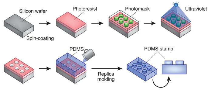
The entire microfabrication process of a common micropatterning is represented in figure 1.
It consists in the combination of two lithography techniques, photolithography and soft-lithography, for the fabrication of a polydimethylsiloxane (PDMS) device.

What is photolithography?
Photolithography, known also as optical lithography, is the key process for microstructure scaffold fabrication. Through the photolithography is possible to create a geometrically defined pattern in a layer of an energy-definable polymer called photoresist. The most widely used photolithography technique employs the UV light to transfer a specific pattern from a photomask to the UV light-sensitive photoresist laid on a rigid substrate.
Usually, with the most common clean-room facility, photolithography is used to prepare molds with negative relief patterns of SU-8 photoresist on a silicon (Si) wafer. The SU-8 is an acid-catalyzed negative photoresist often used for the microfabrication of structures with high aspect/ratio [3].
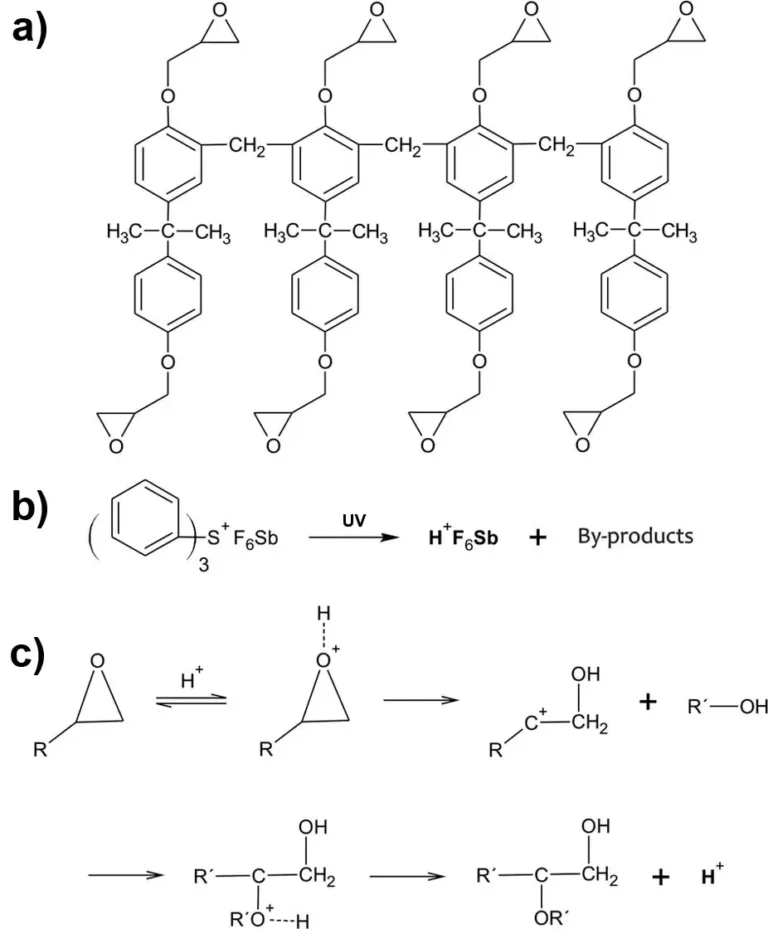
As schematized in figure 2, a uniform film of SU-8 is spin-coated on a Si wafer, then a photomask with a microscale pattern is overlaid and this assembly is exposed to the UV light to transfer the pattern. The photoresist contains indeed highly branched epoxy groups (Fig. 3a) and the UV activates the photolytic reaction by producing the photoacid initiator (Fig. 3b) able to protonate the SU-8 epoxides and start the polymerization (Fig. 3c).
The desired pattern is finally developed by dissolving the uncross-linked photoresist: the precise control of the process allows to achieve the desired micro- and nanoarchitecture in term of dimension, depth and shape. The obtained SU-8 mold presents the inverse pattern of the final device structure and will be used in the following step of soft-lithography.


What is soft-lithography?
Soft-lithography, also called replica molding, uses elastomeric polymers to create stamps complementary to a mold bearing the negative design. This patterning method has several advantages such as lower costs, high throughput, easy setup and good pattern resolution [1].
Once the microfabrication is done by photolithography, the master mold can be used several times to produce the polymer stamps and PDMS, in particular, is the most common elastomer widely employed to create microfluidic devices which find application in different research fields from biology to chemistry and physic.
Figure 4 shows how the PDMS is used in the replica molding to fabricate chips from a SU-8 patterned mold (previously created by photolithography). In particular, a mixture of PDMS base and curing agent is generally poured on the mold and degassed. The PDMS stamp is separated from the mold only after the process of polymerization through a crosslinking at 60 °C for at least 2 h. Finally, in order to obtain the final microfluidic device, the PDMS stamp can be assembled for example with a glass support through a covalent bonding by using the oxygen plasma treatment.

References
[1] Onur, S. et al. 3 – Micro- and nanopatterning of biomaterial surfaces. Fundamental Biomaterials: Metals, Woodhead Publishing, 2018: p. 67-78.
[2] Bhatia, S.N. and D.E. Ingber, Microfluidic organs-on-chips. Nature Biotechnology, 2014. 32: p. 760.
[3] Pinto, C.V., et al., Optimized SU-8 Processing for Low-Cost Microstructures Fabrication without Cleanroom Facilities. Micromachines, 2014. 5(3).
[4] Lima, R.S., et al., Sacrificial adhesive bonding: a powerful method for fabrication of glass microchips. Scientific Reports, 2015. 5: p. 13276.

