In this tutorial, we detail all the steps involved in the manufacture of a microfluidic device, through the example of a double emulsion and trapping chip. This protocol, inspired and extracted from the articles written by Ho, Lee and Liu published in 2016 in Scientific Reports and by Kole et al. published in 2015 in J. Res. Natl. Inst. Stand. Technologie, will give you the keys, from design to microfabrication, to build your own device.
Designing a device
The design presented below has been designed to generate double emulsion droplets.
You can find below a detailed protocol (extracted from Kole et al. published in 2015 in J. Res. Natl. Inst) which will allow you to design a microfluidic device:
1. First of all, it is necessary to use a computer-aided design (CAD) software to design the microfluidic device.
2. Next, we advise you to use the outline of a 100 mm diameter wafer (this obviously depends on the dimensions of your device) and a standard flat as the outer extent of the array device , and pattern device features within center about 90 mm of the wafer to avoid possible edge defects.
3.To manufacture a device with several lithography levels, requiring the application of photoresist to the patterned elements and alignment between subsequent lithography levels, we recommend the following indications :
3.1. You can place the device features, such as the lower alignment marks of the substrate on the first design level. This order is optimal for structuring elements with vertical nanometre dimensions in a flat photoresist film, applied conformally to an unstructured substrate.
If the vertical dimensions of the structured elements in the subsequent photolithography levels are critical, and if the device and array design permits, place the elements on lower levels towards the periphery of the array. This placement will then reduce the variation in the thickness of the centrifugally coated photoresist film on these lower level elements at locations closer to the centre of the wafer where higher level elements will then be placed.
3.2 Next, the lower alignment marks should be placed towards the periphery of the wafer to improve angular alignment and reduce the resulting radial variation in film thickness, and at locations that do not interfere with the characteristics of the device. Ideal placement of the lower alignment marks allows the use of a single strip of linear tape to mask multiple lower alignment marks during centrifugal coating of the photoresist without covering device features. This maintains the visibility of the lower alignment marks while achieving higher levels of photolithography. It is recommended to include at least one pair of lower alignment marks for each higher photolithography level.
3.3. In this third step, you can place device features such as microfluidic channels, inlet and outlet reservoirs, and upper photomask alignment marks on the upper design levels. If the vertical dimensions of these elements are critical, and if the device and die design allows it, then you can place these top level elements closer to the centre of the wafer. This placement will benefit from the reduced variation in film thickness due to the application of a centrifugal photoresist to the lower level elements which are optimally placed towards the periphery of the die. Thus, the lower alignment marks on the substrate should be visible through the upper alignment marks on the photomask, which will mostly be opaque for modelling a mould structure in a negative tone photoresist.
4. Finally, during the photolithography process, you can align the complementary alignment marks through the photomask onto the substrate.
Patterning a device mold
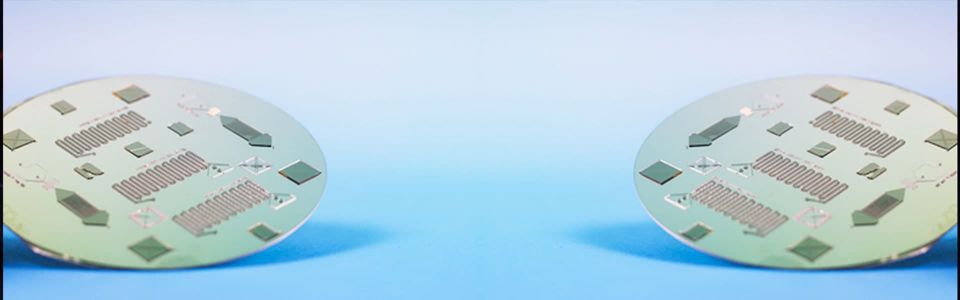
It exist many possible approaches to making a mold for a microfluidic device, using different materials and methods. The most widely used is a photolithographic approach that is ideally suited to rapid prototyping. It consists of centrifugally coating and modelling the SU-8, an epoxy-based negative photoresist, on a silicon wafer. Silicon mold for the top substrate was made by double-layer SU-8 patterning, in which the first patterned layer defines the cross-section of the micropipettes, trapping structures and micro fluidic channel while the second layer defines the trapping structures and main micro fluidic channel. Silicon mold for the bottom substrate was made by single-layer SU-8 patterning, which defines trapping structures and main micro fluidic channel.
Silicon mold for the top substrate
1. The first step consists of a spin-coating of a nanometric film of SU-8 2010 onto a bare silicon wafer.
1.1. To do this, center the silicon wafer on the chuck of a centrifuge with the help of a centering jig.
1.2 Place about 10 ml of SU-8 2010 in the centre of the wafer, taking care not to create air bubbles.
1.3. The first layer of the top substrate, SU-8 2010 is spin coated on silicon wafer at 5000rpm, which gave a thickness of 8 µm.
2.Heat the silicon wafer with a nanometer film of SU-8 2010 at 95° C for 2 min on a hot plate.
3.The first photolithographic exposure of the SU-8 2010 nanometric film must then be carried out.
3.1. To do this, place the silicon wafer with the nanometric film of SU-8 2010 with the first photomask in the contact aligner.
3.2. Place the silicon wafer with the nanometer film of SU-8 2010 and the photomask in soft contact.
3.3. Use an i-line filter to expose the SU-8 2010 nanometric film at a wavelength of 365 nm with a dose of 80 mJ.cm-2.
4.After exposure, re-bake the silicon wafer with the SU-8 2010 nanometric film on a hot plate at 95 °C for 2 minutes.
5.The pattern can now be developed in the exposed nanometer film of SU-8 2010.
5.1. To do this, immerse the silicon wafer with the exposed nanometer film of SU-8 2010 in the SU-8 developer for 1 minute with gentle stirring.
5.2. Then, rinse the silicon wafer with developed features in SU-8 2010 in isopropyl alcohol for 10 s and blow-dry with nitrogen.
6. Bake the silicon wafer with developed features in SU-8 2010 on a hot plate at 150 °C for 30 min. These patterns adhere firmly to the substrate
7. Mask the areas of the silicon wafer with lower alignment marks patterned in the SU-8 2010 using a strip of masking tape with a width of 6 mm (0.25 in) for example. This masking tape will cover the lower alignment marks during the centrifugal coating process. Do not cover areas of the silicon wafer where higher level device features will be patterned as this will prevent photolithography in these areas.
8. It is now possible to spin-coat the second film of SU-8 2010 on the masked silicon wafer with the first patterns of SU-8 2010.
8.1. To do this, center the silicon wafer with SU-8 2010 patterns on the chuck of a centrifuge with the help of a centering jig.
8.2 Place about 10 ml of SU-8 2010 in the centre of the wafer, taking care not to create air bubbles.
8.3 For the second layer, SU-8 2010 is applied with spinning speed of 2000 rpm and gives a total thickness of 15 µm
9. You can now remove the masking tape
10. Bake the wafer with a microscopic film of SU-8 2010 on a hot plate at 95 °C for 8 minutes.
11.Now you can carry out the second photolithographic exposure of the microscopic film of SU-8 2010.
11.1. To do this, place the silicon wafer with the micro-scale film of SU-8 2010 in the contact aligner along with the second photomask for microscale features of the device.
11.2. Align the previously drawn nanometer marks with the microscopic marks on the photomask. Be sure to align the upper and lower alignment marks.
11.3. Place the silicon wafer with the micro-scale film of SU-8 2010 and the photomask into soft contact.
11.4. Use an i-line filter to expose the film of SU-8 2010 at a wavelength of 365 nm with a dose of 160 mJ.cm-2.
12. After exposure, bake the silicon wafer with the exposed microscopic film of SU-8 2010 on the hot plate at 95 °C for 8 minutes.
13. It is now time to develop the pattern in the exposed microscopic film of SU-8 2010.
13.1. To do this, prepare two SU-8 developer containers for a first bulk removal of SU-8 2010, followed by a cleaning rinse.
13.2 Immerse the wafer with the exposed microscopic film of SU-8 2010 in the first container for 45 s with gentle shaking.
13.3 Immerse the wafer with the partially developed microscopic film of SU-8 2010 in the second container with gentle stirring for 30 s.
13.4. Rinse the wafer with a fully developed microscopic film of SU-8 2010 with isopropyl alcohol and dry it with nitrogen.
14. Inspect the resulting device mold by light microscopy. If residues of SU-8 2010 persist, rinse the wafer.
Silicon mold for the bottom substrate
For the bottom substrate, a single layer of SU-8 2010 was patterned with thickness of 15 µm under a spinning speed of 1500 rpm.
It is recomended to measure the film thickness of the patterned elements of the SU-8 2010 using, for example, a scanning probe surface profilometer or an atomic force microscope.
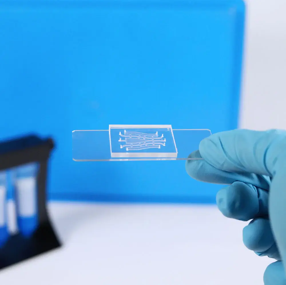
Molding a device
After the silicon molds were fabricated, they were casted with PDMS (Sylgard-184). The control layer was casted in a mixing ratio of 7:1 (base:curing agent). The flow channel membrane was generated by spin-coating PDMS with a mixing ratio of 20:1 on the flow layer silicon mold. Importantly, the PDMS membrane contacts the bottom of the flow channel at 30, 25 and 20 psi for devices with PDMS spin-coating speeds of 1000, 1200 and 1600 rpm respectively. After the PDMS control substrate was diced and punched holes, both the diced PDMS control substrate and the PDMS flow layer membrane on the silicon mold were placed in an oxygen plasma etcher. The diced PDMS control layer substrate was then carefully aligned and bonded with the PDMS flow layer membrane using a customized alignment platform on an optical microscope. A thin PDMS membrane separates the microfluidic channel and the control layers that serve two different functions and are independently controlled. To direct flow to the trapping chambers, a pneumatically controlled valve set located above the microfluidic channel blocks the flow in the main microfluidic channel when the valve set is actuated. A second control valve set directly above the trapping chambers exerts compression to trapped double emulsion when the valve set is actuated. Since the two control valve sets can be independently controlled, trapping is decoupled from compression. Finally, the PDMS substrate was bonded to this glass slide.
Glass capillary microfluidic device was fabricated by assembling tapered round capillary, square capillary and syringe needles together using 5 minutes epoxy. First, the round glass capillary was pulled using a pipette puller. The tapered capillary was then sanded using 1200 grade sandpaper to obtain a 100 μ m opening for the collection tube. The outside surface of a clean 15 μm opening injection tube, pulled and similarly sanded, was treated with trichloro(1H,1H,2H,2H-perfluorooctyl)silane to render the surface hydrophobic. Then, the injection tube and collection tube were inserted into a square capillary placed on a glass slide and they were aligned under an optical microscope. Syringe needles were cut and glued to the glass slide using 5 minutes epoxy. Lastly, micro-tubings were connected to the syringe needles.
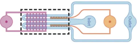
Trapping of double emulsions
Double emulsions were trapped inside the microfluidic device for the application of mechanical forces. Double emulsions with a diameter between 40 μm and 90 μm were first generated in a glass capillary microfluidic device and then reinjected into the microfluidic device at 10x dilution. To trap double emulsions in the trapping chambers, Control valve set 1 was then pressurized at 10 – 15 psi to block the main microfluidic channel, which increased the flow resistance in the main microfluidic channel. The flow resistance ratio between the microchannels and the main microfluidic channel will reduce and more fluid streamlines will go through the microchannels.
This greatly increases the trapping efficiency of the double emulsions and it is possible to find all 14 trapping chambers filled up within a minute. A double emulsion will be trapped if the radius of the double emulsion is smaller than the instantaneous critical stream width, which is dictated by the flow resistance ratio between the micropipette and main microfluidic channel.